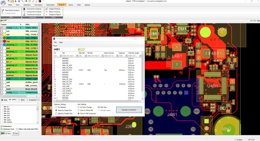
When reverse engineering PCB board, component placement and connection must be taken into consideration, before connecting component leads, first extract the solder joints and wiring information from the database, and then automatically place solder joints and wires on the PCB scanning image through bare PCB board. If there are no relevant solder joints and wiring information in the database, you need to manually place the solder joints and wires on the PCB scanning image. After the solder joints and wires are placed, the components are placed against the PCB image to fulfill Component Pin Connection Functional Analysis.

Arranging components also requires other auxiliary functions to improve component placement efficiency. Importing the PCB board scanning image is the first step in drawing the component layout.
“Loading the board image and loading the front and back sides of the PCB board image” as the 1st step for image processing and recognition. After loading, the two images are coincident, that is, the through holes are in the front and back. The relative coordinates are the same to solve the positioning problem of the front and back of the printed circuit board. When the front hole is arranged, the same through hole can be placed on the opposite side.
“Importing solder joints and wires” is to export the solder joints and wires on the PCB board from the database. Since there are many solder joints and wires on the circuit board, the manual solder joints and wires are quite cumbersome and time consuming. Therefore, it is necessary to realize the automatic placement of solder joints by image recognition technology. After image recognition, the relevant position information of the solder joints and the connection lines are recorded into the database. Before the components are arranged, relevant information is read from the database and displayed on the board image. Draw solder joints and connections at the corresponding locations.


