One of the most and advanced step to reverse engineering PCB board is Collecting Reverse Engineered Circuit Board Data mainly includes the following:
(1) Take all-round photos of targered printed circuit board that require reverse engineered design, so as to record the installation positions of all components which include capacitor, resistor, inductors, etc, which is convenient for copying PCB board’s layout diagram and duplicating printed circuit board in the future, to avoid unnecessary errors.
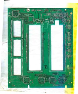
(2) Remove all devices (as shown in below Figure). When removing devices, below rules must be strictly followed:

desolder off components from PCB board when reverse engineering it
①Strict attention to personal safety is required (the temperature of the disassembly tool is high). Generally, an electric soldering iron for plug-in components is usually used. For BGA packages, SMD devices, flip chips, etc., special equipment is required to disassemble PCB board parts, otherwise, very It is easy to damage the desoldered parts and the circuit board;
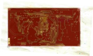
② The protection over the surface of printed circuit board shall not damage the board surface. After the device is disassembled, you need to use a camera or scanner to record the board surface and save it in BMP or JPG picture format.

After the device is disassembled, you need to use a camera or scanner to record the board surface and save it in BMP or JPG picture format
When using related equipment to record on the board, make sure that the electronic PCB card is placed horizontally and vertically without tilting. When taking pictures, pay attention to the camera and the board parallel to each other.
The problem of reverse engineering PCB board accuracy is very important. It affects the accuracy and quality of line width copying. It mainly depends on the accuracy of the original scanned image. Based on experience, it is best to choose a higher DIP when scanning.


