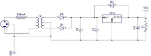
When Cloning Power Supply Circuit Board Gerber File, the layout of the components should be compact, all the connections should be kept as short as possible, and the components and wiring should be laid out according to the functional relationship of the components in the Power Supply Circuit Board schematic diagram.
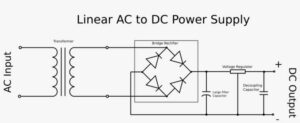
In this power supply pcb board diagram, rectification is performed first, followed by filtering. After filtering, the voltage is stabilized. After the voltage is stabilized, the energy storage capacitor flows through the capacitor before power is used for the subsequent circuits.

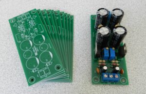
linear power supply PCB diagram of the above schematic
In the above Figure is the PCB diagram of the above schematic, and the two diagrams are similar. The wiring on the left and the right is a bit different. The power supply in the left picture is rectified and directly reaches the input pin of the voltage regulator chip, and then the voltage regulator capacitor. The filtering effect of the capacitor here is much worse. The output There are also problems.

Clonación del archivo Gerber de la placa de circuito impreso de la fuente de alimentación
The picture on the right is a better picture. We must not only consider the flow direction of the positive power supply, but also the ground return problem. Generally speaking, the positive power supply line and the ground return line should enter and exit at the same time as much as possible, and should be as close to each other as possible.

Power Supply Circuit Board schematic diagram copying
When Cloning Power Supply Circuit Board Gerber File, you should also pay attention to the heat dissipation problem of the power regulator chip of the linear power supply. How does the heat come from? There is a voltage drop of 5V, and the heat generated is 2.5W; If the input voltage is 15V, the voltage drop is 10V, and the heat generated is 5W. Therefore, we need to reserve enough heat dissipation space or reasonable heat sinks according to the heat dissipation power. Linear power supply is generally used in occasions where the voltage difference is relatively small and the current is relatively small, otherwise, please use a switching power supply circuit board cloning technique;


