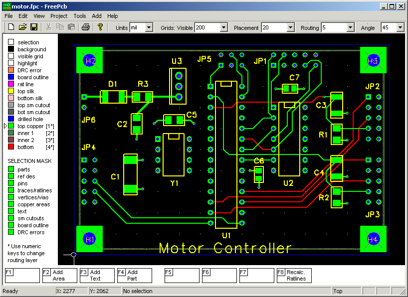
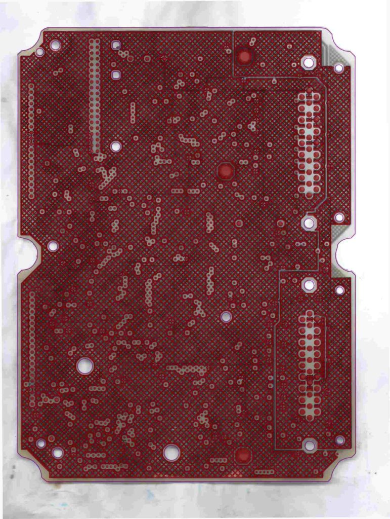
Cloning PCB Circuit Board Ground Design drawing can effectively help to anti-noise which generate in the PCB board layout design;

A. The digital ground is separated from the power ground.
If there are both logic circuits and linear circuits on the line, they should be separated as much as possible. The ground of the low-frequency circuit should use a single point and connect the ground as much as possible. When the actual printed circuit board re-wiring is difficult, it can be partially connected in series and then connected in parallel. High-frequency pcb circuit board should use multi-point serial connection ground. The ground wire should be short and thick. Large-scale grid-like copper should be used around high-frequency components.
B • The ground wire should be thickened as much as possible. If the grounding wire uses a very thin wire, the grounding potential changes with the change of the current, so that the anti-noise performance is reduced.

Therefore, the grounding wire should be thickened so that it can pass three times the allowable current on the printed circuit board. If possible, the ground wire should be above 2 ~ 3tntn.
C. The ground wire constitutes a dead-loop circuit. A printed circuit board composed only of digital circuits. The ground circuit is arranged as a dead-loop circuit. It can greatly improve the ability to resist noise.
- 2 Power cord design
A. According to the power consumption of the printed circuit board, the width of the power line should be thickened as much as possible to reduce the loop resistance. At the same time, the direction of the power supply line and the ground line and the direction of data transmission are consistent, which helps the ability to resist strong noise


