When we cloning PCB board, the component symbol will be designed in a specific way to opt for the clone double layer printed circuit board procedures:
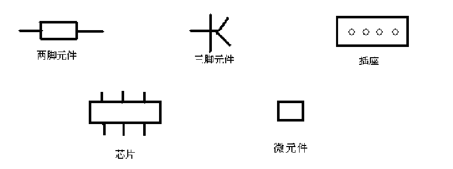
One type of component with two pins is called a two-legged component, such as a diode, a capacitor, an inductor, etc. A type of component that has only three pins is called a tripod component, such as a triode.
Some small components with tiny size that do not know the pin count are called microcomponents. Others and so on. In addition, the through-hole, half-hole, and pad line segment bifurcation points are collectively referred to as solder joints.
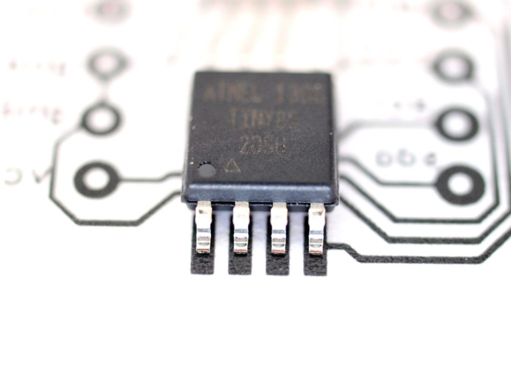
In summary, all components can be divided into two categories: two-legged components, three-legged components, chips, switch sockets, and micro-components. The basic patterns of the five categories are shown in below figure:

Each component graphic has some basic deformation depending on the original physical image. The symbol graphic of the component can be represented either by a bitmap or by a vector diagram. Bitmaps show better visual effects and easier control, but they also take up more storage space, which can cause distortion of the graphics.

Vector graphics are mainly composed of lines and color blocks, which can be decomposed into individual graphic elements such as single lines, text, circles, rectangles, and polygons. The details in the vector enlargement graph are not distorted, and the files after saving are smaller than the same bitmap, as a result of that, we can have a better performance by using vector graphics than bitmaps when design the component symbom of PCB reverse engineering;


