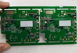
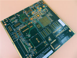
When Cloning Multi-layer Backplane PCB Board, one of the most basic issues to consider is how many layers, ground planes and power planes are needed to achieve the functions required by the circuit, and the number of layers of the PCB board layers, ground planes and power planes is determined.

Cloning Multi-layer Backplane PCB Board, one of the most basic issues to consider is how many layers, ground planes and power planes are needed to achieve the functions required by the circuit
The use of decoupling capacitors is an important measure to address power integrity. Decoupling capacitors should only be placed on the top and bottom layers of the PCB. The traces, pads, and VIAs of the decoupling capacitors will seriously affect the effect of the decoupling capacitors. This requires that the traces connected to the decoupling capacitors should be as short and wide as possible, and the wires connected to the VIAs should also be as short as possible.

in a high-speed digital circuit board design cloning, decoupling capacitors can be placed on the top layer of the PCB, with layer 2 assigned to the high-speed digital circuit (such as a processor) as the power plane, layer 3 as the signal layer
For example, in a high-speed digital circuit board design cloning, decoupling capacitors can be placed on the top layer of the PCB, with layer 2 assigned to the high-speed digital circuit (such as a processor) as the power plane, layer 3 as the signal layer, and layer 4 as the signal layer. Set to high-speed digital circuit ground. In addition, try to ensure that the signal traces driven by the same high-speed digital device use the same power supply layer as the reference plane, and this power supply layer is the power supply layer of the high-speed digital device.


