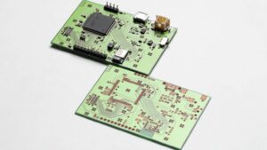
One of the purpose of Cloning Electronic PCB Circuit Board Layout Design is to optimize Wiring pattern and silk screen placement.
“PCB d
esign is not the best, only better”, “PCB design is an art of defects”, this is mainly because original PCB board layout design needs to realize the design requirements of all aspects of hardware, and individual requirements may be in conflict. Bear’s paw and fish cannot have both.

One of the purpose of Cloning Electronic PCB Circuit Board Layout Design is to optimize Wiring pattern and silk screen placement.
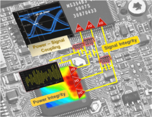
For example: a multilayer printed circuit board reverse engineering project needs to be designed as a 6-layer board after the circuit board designer’s evaluation, but the product hardware must be re-designed as a 4-layer printed circuit board layout due to cost considerations, so the signal shielding layer can only be sacrificed, resulting in adjacent wiring the signal cross-talk between layers increases and the signal quality decreases.

a multilayer printed circuit board reverse engineering project needs to be designed as a 6-layer board after the circuit board designer’s evaluation, but the product hardware must be re-designed as a 4-layer printed circuit board layout due to cost considerations
The general pcb circuit board layout design cloning experience is: the time to optimize the wiring is twice the time of the first wiring. After the PCB layout optimization is completed, post-processing is required.
The first thing to do is the silk screen logo on the PCB surface. The bottom silk screen characters need to be mirrored during design to avoid confusion with the top silk screen.


