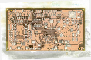
When we Cloning Electronic PCB Board Gerber File, the accuracy is the most important thing to be concerned, since the circuit board reproduction success will greatly depends on it, as a result of that, we will have chance to make errors in the process of reverse engineering PCB board,
There are two main possibilities:
1, When the circuit board is scanned, the electronic circuit board cannot be placed horizontally and vertically. In such cases, the circuit board needs to be rescanned;

Cloning Electronic PCB Board Gerber File, SCHEMATIC and BOM list
2, It is normal for the two pictures to automatically overlap with errors. First select the circuit layer, And then make small movements so that the two layers completely overlap each other;
As can be seen from Figure 6, the current circuit layer blocks the top surface, so there is no way to copy electronic pcb board, so the circuit layer needs to be hidden, and the pads and vias in the circuit layer must be able to be left, because the common parts of the two layers in the double panel are pads and vias. Open the layer property setting dialog box, and tick the bottom layer of the line layer.
Repeat the second step to place the wire and copper surface
As can be seen, this is a double-sided board with two signal layers but no components. At this time, the package form of components can be placed on the character layer (the data collection part has been requested to be prepared in advance) , This step can also be carried out in CAD software design. Then save it as test.pcb (the file type is Protel2.8pcb files).
Use the CAD software Protel 99se to open the test.pcb file and add components with reference to the template, Prohibit the setting of the wiring layer.


