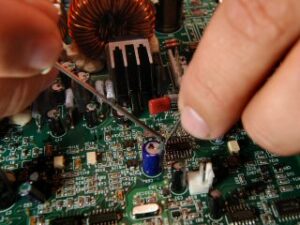
In the original electronic printed circuit board especially when re-routing multi-layer PCB board layout design, the hot spot must be avoid since signal vias will generate voids on the power layer and bottom layer. Therefore, unreasonable placement of vias is likely to increase the current density in certain areas of the printed circuit board power supply or ground plane reverse design.

Clone PCB Circuit Card Gerber File Vias
These areas where the current density increases are called hot spots. Therefore, we must try our best to avoid this situation when setting the vias in the process of cloning printed circuit borard layout design, so as to prevent the plane from being split, which will eventually lead to EMC problems.
Usually the best way to avoid hot spots is to place vias in a mesh pattern of circuit board, so that the current density is uniform, and the planes will not be isolated at the same time, the return path will not be too long, and EMC problems will not occur.


