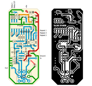
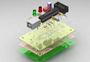
Clone Obselete Circuit Board Design Schematic needs to consider including electronic PCB card structure design and electronic PCB card relayout drawing;
According to the determined circuit board size and various mechanical positioning, redraw the PCB frame in the PCB design environment, and place the required connectors, buttons/switches, screw holes, assembly holes, etc. according to the positioning requirements.

Clone Obselete Circuit Board Design Schematic
Fully consider and determine the wiring area and non-wiring area (such as how much area around the screw hole belongs to the non-wiring area)
PCB layout design
The PCB layout design is to place the devices in the PCB frame according to the design requirements. Generate the net-list in the schematic tool (Design→Create Netlist), and then import the netlist in the PCB software (Design→Import Netlist).
After the Printed circuit board netlist is successfully cloned, it will exist in the background of the software. Through the Placement operation, all devices can be called out, and there is a flying line prompt connection between the pins.

After the Printed circuit board netlist is successfully cloned, it will exist in the background of the software. Through the Placement operation, all devices can be called out, and there is a flying line prompt connection between the pins
At this time, the layout design of the device can be carried out. PCB layout design is the first important process in the entire Obselete Circuit Board Design Schematic cloning process. The more complex the PCB board, the better the layout can directly affect the difficulty of later re-wiring.
The layout design relies on the circuit board designer’s basic circuit knowledge and rich design experience, which is a higher level requirement for the circuit board designer. The junior circuit board designer has little experience and is suitable for small module layout design or PCB layout design tasks with lower difficulty of the whole board.


