When we clone multilayer PCB board stackup structure, first needs to determine the number of layers of the multilayer PCB board, the next step is to properly arrange the placement order of each one of the layers. In this step, there are two main factors to consider:

The distribution of special signal layers.
Distribution of power and ground layers.
If the number of layers of multilayer PCB board is larger, the combinations of special signal layers, ground layers and power layers are more difficult. How to determine which combination is optimal will become more difficult, but the general principles are as follows:
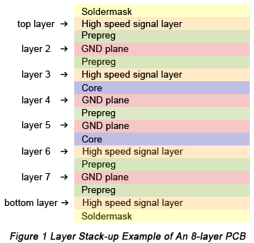
The signal layer should be adjacent to an internal electrical layer (internal power/ground), using a large copper foil of the inner layer to provide shielding for the signal layer.

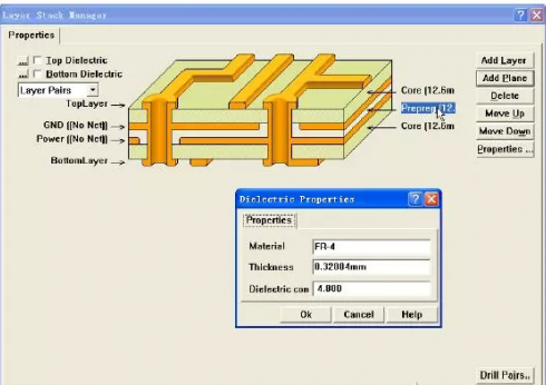
The internal power supply layer and the ground plane should be tightly coupled, that is, the dielectric thickness between the internal power supply layer and the ground layer should be set to a small value to increase the capacitance between the power supply layer and the ground layer, and increase the resonant frequency. The media thickness between the internal power plane and the ground plane can be set in Protel’s Layer Stack Manager.
Select the [Design] / [Layer Stack Manager] command, the system pops up the layer stack manager dialog box, double-click the Prepreg text with the mouse, and the dialog box shown in below Figure pops up, you can change the insulation in the Thickness option of the dialog box. The thickness of the layer.

If the potential difference between the power supply and the ground is not large, a smaller insulation thickness, such as 5 mils (0.127 mm), can be used.
The high speed signal transmission layer in the pcb circuit should be the signal intermediate layer and sandwiched between the two inner layers. The copper films of the two inner layers can provide electromagnetic shielding for high-speed signal transmission, and can also effectively limit the radiation of high-speed signals between the two inner layers without external interference.
Avoid two signal layers directly adjacent. Crosstalk is easily introduced between adjacent signal layers, resulting in failure of circuit functions. so when cloning the multilayer pcb board inner layer, adding a ground plane between the two signal layers can effectively avoid crosstalk.
Multiple grounded internal layers can effectively reduce the ground impedance. For example, the A signal layer and the B signal layer use separate ground planes, which can effectively reduce common mode interference, designer can apply multiple ground internal layer on the PCB gerber file acquired from PCB reverse engineering.


