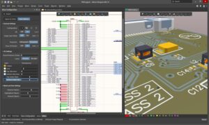
To put it bluntly, Clone Electronic PCB Circuit Board Layout Diagram is to recreate printed circuit board’s circuitry pattern and netlist drawing according to physical PCB board sample, this is a quite useful technique especially for electronic device pcb board reproduction;

Clone Electronic PCB Circuit Board Layout Diagram is to recreate printed circuit board’s circuitry pattern and netlist drawing according to physical PCB board sample, this is a quite useful technique especially for electronic device pcb board reproduction
the layout is to put devices on the circuit board. At this time, if all the preparations mentioned above are done, you can generate it on the cloned PCB schematic net-list (Design->Create Netlist), and then import the netlist (Design->Load Nets) on the PCB diagram.
Just saw the devices are all piled up, and there are flying wires between the pins to indicate the connection. Then you can clone the layout the circuit board.

General layout press Proceed with the following principles:
1. According to the reasonable division of electrical performance, it is generally divided into: digital circuit area (fear of interference and interference), analog circuit area (fear of interference), Power drive area (interference source);
2. Circuits that complete the same function should be placed as close as possible, and each component should be adjusted to ensure the most concise connection; at the same time, adjust each function The relative position between the blocks makes the connection between the function blocks the most concise;


