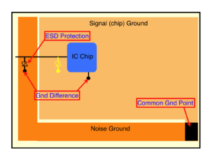
When we Clone Electronic PCB Board Layout Design which will normally refers to redraw printed circuit board gerber file, through which can to improve the ESD performance of the whole circuitry system, and in order to realize the purpose, below measure must be taken:
1st of all, Put all connectors aside if possible, if possible, lead the power cord from the center of the electronic circuit card and away from areas that are directly affected by ESD.

When we Clone Electronic PCB Board Layout Design which will normally refers to redraw printed circuit board gerber file, through which can to improve the ESD performance of the whole circuitry system
On all PCB layers below the connector leading out of the chassis (easy to be directly hit by ESD), place a wide chassis ground or polygon-filled ground, and connect them together with vias at intervals of approximately 13mm.
Place mounting holes on the edge of the PCB card, and use solderless top and bottom pads around the mounting holes to connect to the chassis ground.
During PCB assembly cloning, do not apply any solder to the top or bottom pads. Use screws with embedded washers to achieve close contact between the PCB and the metal chassis/shield or support on the ground plane.
Between the chassis ground and circuit ground of each layer, the same “isolation area” should be set; if possible, keep the separation distance at 0.64mm. At the top and bottom layers of the card near the mounting holes, every 100mm along the chassis ground The wires connect the chassis ground and the circuit ground with 1.27mm wide wires.
Adjacent to these connection points, place pads or mounting holes for mounting between the chassis ground and the circuit ground. These ground connections can be cut with a blade to maintain an open circuit, or jumpers with magnetic beads/high-frequency capacitors.
If the circuit board will not be placed in a metal chassis or shielding device, solder mask should not be applied to the top and bottom chassis grounds of the circuit board, so that they can be used as discharge electrodes for ESD arcs.


