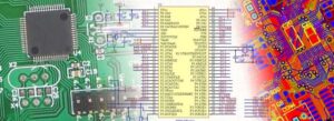
Clone Electronic Circuit Board Gerber File have some items need to be taken care, below points will refer to how to extract layout and schematic diagram from a physical PCB board properly and place components onto the right position:

Clone Electronic Circuit Board Gerber File have some items need to be taken care, below points will refer to how to extract layout and schematic diagram from a physical PCB board properly and place components onto the right position
The distance between BGA and adjacent components>5mm.
The distance between other SMD components>0.7mm; the distance between the outside of the mounting component pad and the outside of the adjacent interposing component is greater than 2mm;
PCB with crimping parts, no interposing within 5mm of the crimped connector Components and devices shall not be mounted within 5mm of the welding surface.
1. The layout of the IC decoupling capacitor should be as close as possible to the power supply pin of the IC, and the loop between it and the power supply and ground should be the shortest.
2. In the component layout, appropriate consideration should be given to placing the devices using the same power supply as close together as possible to facilitate future power supply separation.
3. The layout of the resistance vessel for impedance matching purposes should be arranged reasonably according to its properties. The layout of the series matching resistor should be close to the driving end of the signal, and the distance generally does not exceed 500 mil. The layout of matching resistors and capacitors must distinguish the source and terminal of the signal. For multi-load terminal matching, it must be matched at the far end of the signal.
4. After the layout is completed, print out the assembly drawing for the schematic designer to check the correctness of the device package, and confirm the signal correspondence between the single board, the backplane and the connector, and the wiring can be started after confirmation.


