Double Layer Printed Circuit Board is the most commonly used type of PCB board in the electronic world, refers to the industries we most serve which from industrial to automobile, hereby we would like to introduce the standard procedure of Clone Double Layer Printed Circuit Board:
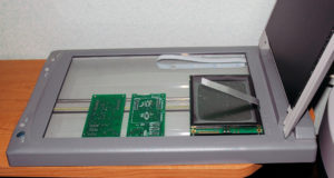
1. Scan the top and bottom layer of the printed circuit board and save as TOP.BMP & BOT.BMP pictures

scan pcb board top layer
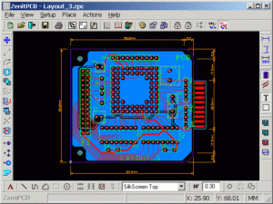
2. Open the PCB designing software Quickpcb2005, click “File”, “Open Basemap”, and open a scanned image. Use PAGEUP to magnify the screen, see the pad, place a pad according to PP, and draw PT trace from the line… draw it again in this software, click “save” to generate a B2P file

edit pcb pictures by software
3. Then click “File” “Open Basemap” to open another layer of the scanned image;
4. Click “File” “Open” to open the previously saved B2P file. We can see that the target printed circuit board is stacked on top of this picture – the same PCB board, the hole is in the same position, but the line connection is different. . So we press “Options” – “Layer Settings” to turn off the display and silkscreen of the top layer here, leaving only VIAs of multiple layers;
5. The VIAs in the top layer are in the same position as the VIAs in the bottom image. We can trace the bottom lines. Then “save” – the B2P file now has the PCB layout drawing includes top and bottom two layers.
6. Click “File”, “Export to PCB file”, you can get the PCB layout drawing with two layers, then the PCB board layout drawing can be modified or reverse engineering the schematic diagram and directly send to manufacturer for Clone Double Layer Printed Circuit Board.


