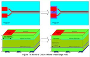
The impedance value of a trace generally depends on its line width and the distance between the trace and the reference plane, and impedance is more likely to generated in the High Density Interconnect PCB board layout, engineer must pay special attention when Clone HDI PCB board to avoid discoutinuous impedance issue.

impedance is more likely to generated in the High Density Interconnect PCB board, engineer must pay special attention when Clone HDI PCB board to avoid discoutinuous impedance issue
The wider the trace, the lower its impedance. In some interface terminals or pads of printed circuit board, the principle is also applicable. When the pad of an interface terminal is connected to a high-speed PCB board signal line, if the pad is particularly large at this time, and reverse engineering high-speed PCB board signal line is particularly narrow, the impedance of the large pad is small, and the narrow trace must have a large impedance.
In this case, impedance discontinuity will occur, and signal reflection will occur if impedance is discontinuous. Therefore, in order to solve this problem in the process of cloning hdi pcb board, a forbidden copper sheet is placed under the large pad of the interface terminal or device, and the reference plane of the pad is placed on another layer to increase the impedance to make the impedance continuous.
Vias are another source of impedance discontinuity. In order to minimize this effect, the unnecessary copper skin connected to the inner layer and the via should be removed. In fact, such an operation can be eliminated by CAD tools or contact the PCB processing manufacturer to eliminate unnecessary copper during circuit board layout redesign, and ensure the continuity of impedance.

Vias are another source of impedance discontinuity


