Altium Design PCB Tool Place Components and Borders Accurately, In our usual cognition, dimensioning is mostly used in PCB production and PCB board assembly files cloning to mark the dimensions of components and frames. Generally, it is customary in the PCB layout design process to draw a PCB board before dimensioning deal with.

Altium Design PCB Tool Place Components and Borders Accurately
But in fact, another way of thinking is to consider, we can use size to accurately place components and draw borders.
Using Altium Designer for reverse engineering pcb board profile and outline, it is estimated that 80 to 90% of my friends will be able to do so. I will not say much here. It is just an operation as a brief introduction to the method of drawing borders by size.
First of all, let’s draw a quadrilateral at random. A brief introduction is really rough. Let’s just use a quadrilateral for the border.
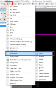
Call up the dimensioning tool, Place>>Dimension>>Linear, as shown in image 2:

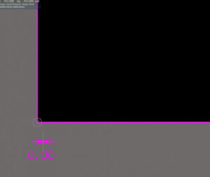
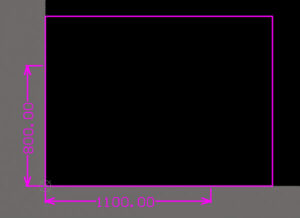
At this time, carry out the dimensioning. Note that it is not the dimensioning of the frame that I have drawn! ! The size marked should be the size of pcb board we intend to redraw! Of course, the starting point we choose should be consistent.


As you can see from Figure 4, how ridiculously poor the border I drew is.
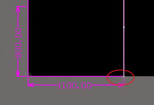
Next, let’s adjust the border to the correct position. First pull the one on the right to the position of the dimension mark. Don’t be afraid of being inaccurate. When you pull it back, go to the vertical rod marked below, and the center of the cross will be aligned. As shown in below Figure:


