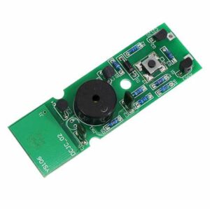
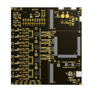
When Reverse Engineering a Controller PCB Circuit Board, one of the most basic issues to consider is how many circuitry wiring layers, ground planes and power planes are needed to achieve the functions required by the circuit system, and the number of layers of the printed circuit board wiring layers, ground planes and power planes is determined related to circuit function, signal integrity, EMI, EMC, manufacturing cost, etc.

reverse engineering a controller pcb circuit board
For most PCB board cloning designs, there are many conflicting requirements such as PCB performance requirements, target cost, manufacturing technology and system complexity. PCB stack-up design is usually a compromise decision after considering various factors. High-speed digital circuits and whisker circuits are often designed with multilayer PCB boards.

For most PCB board cloning designs, there are many conflicting requirements such as PCB performance requirements, target cost, manufacturing technology and system complexity.
In a multi-layer PCB board cloning, there are usually signal layers (S), power (P) planes and ground (GND) planes. Power and ground planes are usually undivided solid planes that will provide a good, low-impedance current return path for current from adjacent signal traces. Signal layers are mostly located between these power or ground reference plane layers, forming either symmetrical striplines or asymmetrical striplines. The top and bottom layers of a multi-layer PCB are usually used to place components and a small number of traces. These signal traces are not required to be too long to reduce the direct radiation generated by the traces.


