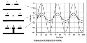
When we talk about Low Frequency Analog Signal Package Grounding in the PCB board ground gerber file redrawing, let’s look at the size of the cross-talk in the case of the surface microstrip line.
Assuming that the trace is controlled by 50Ω impedance, the line width is 6mil, the dielectric thickness is 3.6mil, and the dielectric constant is 4.5. And suppose that the two signals are analog signals with a carrier frequency of 30Mhz and a bandwidth of 2Mhz.
The following figure shows the far-end cross-talk in three cases. When the line spacing is 6mil, because the two lines are tightly coupled, the far-end crosstalk is larger. Increasing the spacing to 18 mils significantly reduces the far-end crosstalk.

Low Frequency Analog Signal Package Grounding
Furthermore, a protective ground wire is added between the two wires, and both ends of the ground wire are connected to the ground with via holes, and the far-end cross-talk is further reduced. For isolation between low-frequency analog signals, the protective ground wire is indeed very useful. This is also the reason why many low-frequency printed circuit board drawing cloning often see “landing”.
However, if an isolated digital signal is required, the situation will be different. We divide the surface microstrip line and the inner strip line to discuss the isolation effect of the protective ground line on the digital signal. In the following discussion, I did not assume that the PCB traces are all controlled by 50Ω impedance.


