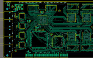
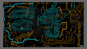
When we Reverse Engineering High Speed PCB Board Layout Diagram, for high-speed digital signals, a 90° corner will have a certain impact on high-speed signal transmission lines.
For our current high-density high-speed PCBs reverse engineering, the general trace width is 4-5mil, and the capacitance of a 90° corner is about 10fF. It is estimated that the cumulative delay caused by this capacitance is about 0.25ps, so the 90° corner on the 5mil line width wire will not have a great impact on the current high-speed digital signal (100-psec rising edge time).

Reverse Engineering High Speed PCB Board Layout Diagram
For high-frequency signal transmission lines, in order to avoid signal damage caused by the skin effect, a wider signal transmission line is usually used, such as 50Ω impedance and 100mil line width. The line width at the 90° corner is about 141mil, the signal delay caused by parasitic capacitance is about 25ps.

microwave transmission lines always hope to reduce signal loss through reverse engineering PCB board design
At this time, the 90° corner will have a very serious impact, at the same time, microwave transmission lines always hope to reduce signal loss through reverse engineering PCB board design as much as possible. Impedance discontinuities at 90° corners and parasitic capacitance outside will cause phase and amplitude errors of high-frequency signals, mismatches between input and output, and possible parasitic coupling, in turn, leads to the deterioration of circuit performance and affects the transmission characteristics of PCB circuit signals. Regarding the 90° signal routing, our view is to avoid 90° routing as much as possible.


