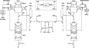
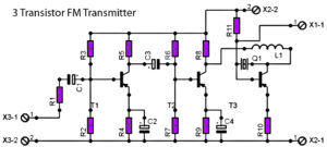
The main application area of radio frequency circuits is wireless communication, through our RF PCB board reverse engineering technique, we can Clone RF Circuit Board Schematic Diagram. Below Figure is a block diagram of a typical wireless communication system. The following uses this system as an example to analyze the role of radio frequency circuits in the entire wireless communication system for pcb circuit card cloning.

The main application area of radio frequency circuits is wireless communication, through our RF PCB board reverse engineering technique, we can Clone RF Circuit Board Schematic Diagram.
This is a system model of a wireless communication transceiver (transceiver), which includes a transmitter circuit, a receiver circuit, and a communication antenna. This transceiver can be used in personal communications and wireless local area networks.
In this system, the digital processing part is mainly to process digital signals, including sampling, compression, encoding, etc.; and then through the A/D converter into an analog form to enter the analog signal circuit unit. The analog signal circuit is divided into two parts: the transmitting part and the receiving part.

the digital processing part is mainly to process digital signals, including sampling, compression, encoding, etc.; and then through the A/D converter into an analog form to enter the analog signal circuit unit.
The main function of the transmitting part is: the low-frequency analog signal output by the digital-to-analog conversion and the high-frequency carrier provided by the local oscillator are up-converted into a radio frequency modulated signal through the mixer, and the radio frequency signal is radiated into the space through the antenna.


