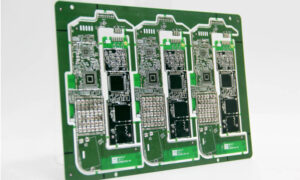
Clone Electronic PCB Card Layout Design needs to pay attention to below points, which will ensure the electrical integrity and functionality compatibility in the reverse engineering printed circuit board schematic:

clone electronic pcb card layout design
Several basic principles: any wire in the electronic pcb card layout design has impedance; current always automatically selects the path with the least impedance; radiation intensity is related to current, frequency, and loop area; common mode interference is related to the mutual capacitance of large DV/DT signals to ground ; The principle of reducing EMI and enhancing anti-interference ability is similar.
The restored pcb board layout should be partitioned according to power supply, analog, high-speed digital and each functional block. Minimize the area of the large di/dt loop and reduce the length (or area, width of the large dv/dt signal line). The increase in the trace area of PCB board cloning will increase the distributed capacitance. The general approach is: the width of the trace try to be as large as possible, but remove the excess part), and try to walk in a straight line to reduce the hidden area to reduce radiation.
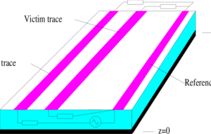
Inductive crosstalk is mainly caused by the large di/dt loop (loop antenna), and the induction intensity is proportional to the mutual inductance, so it is more important to reduce the mutual inductance with these signals (the main way is to reduce the loop area and increase the distance);
Capacitive crosstalk is mainly produced by large dv/dt signals of printed circuit board design, and the induction intensity is proportional to the mutual capacitance. All decrease the mutual capacitance with these signals (the main way is to reduce the effective coupling area and increase the distance. The mutual capacitance increases with the distance decrease faster) is more critical.


