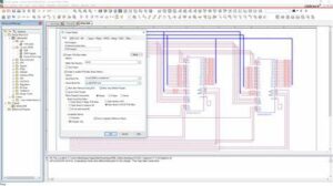
How is Reverse Design A Better PCB Board Schematic Diagram to realize a better and more reliable performance over electronic device has become a strong request for most of the electronic engineers, hereby we will introduce two ways for it:
first of all, Name the circuit network, network is playing an critical role in the whole process of printed circuit board cloning engineering, with it the whole structure of printed circuit board structural design will become easier.

Name the circuit network, network is playing an critical role in the whole process of printed circuit board cloning engineering,
Indeed, there may be doubts about this step, but making sure to name each network on the PCB and mark the purpose of each network can provide you with a lot of help at a critical juncture. It is also useful when you have to debug or run simulations. Network naming allows you to know where to start when something goes wrong. Remember: make the name easy to identify; make the meaning of the name clear at a glance.

Reverse Design A Better PCB Board Schematic Diagram
Take notes
When it comes to electronic circuit board design cloning, your notes are your panacea. It is important to record every step of the printed circuit board re-development process, every pit you encounter, every solution you find, and any other content related to your design. Be sure to note why certain components were selected for your design, the style of logic tables, and any special considerations when designing circuits.
There are many uses for your notes:
• By clearly recording each step, you can “play it back” and see where problems might go wrong or where you can make changes to get a more efficient design.
• You can use and cross-reference comments from previous projects to better understand, implement better solutions, and stimulate more inspiration related to your current work.
• You can help others solve their printed circuit board schematic diagram design problems and read their notes later when needed.


