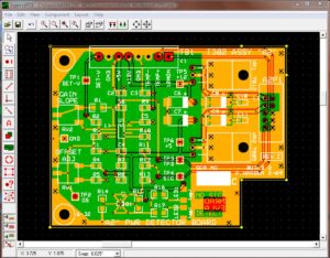
Antenna RF Multi-layer PCB Board Layout Reverse Engineering refers to redraw printed circuit board’s wiring layout redrawing, component list making and schematic diagram restoration;

Antenna RF Multi-layer PCB Board Layout Reverse Engineering refers to redraw printed circuit board’s wiring layout redrawing, component list making and schematic diagram restoration;
The Radio Frequency signal line impedance of the two antenna interfaces needs to be controlled to 50Ω. In practical applications, other parameters of the PCB, such as reference layer thickness, number of layers, and stacking, will affect the RF routing method. In different situations, the reference GND layer is different, and the routing gap will also be large.

70% of the electric field between the lines can be kept without mutual interference, which is called the “3W principle”
When redesigning antenna RF signals on a multi-layer board layout drawing, the first consideration is to meet the basic “3W principle”. In order to reduce the crosstalk between the lines, the line spacing should be large enough. If the line center distance is not less than 3 times the line width, 70% of the electric field between the lines can be kept without mutual interference, which is called the “3W principle”.


