In Printed circuit board layout redesign, we will be involved in the PCB board BOM list sorting. For what components a circuit board needs to use, what package, component type, attribute, and even manufacturer, these information will be sorted into a BOM List which can be built through PCB reverse engineering.
It would be tedious and time-consuming to organize the BOM list manually. Fortunately, the general PCB reverse engineering drawing software integrates the function of automatically generating BOM.
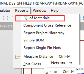
Today we will talk about how to flexibly use the BOM report in the Altium Designer software to organize the component information we need.

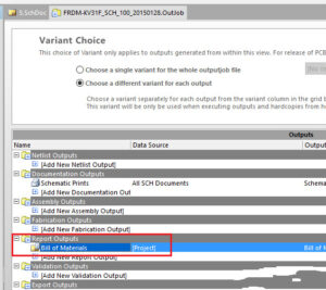
Or you can find the location of bom in the location shown in Figure 2:

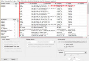
As shown in above Figure 3, the red box on the upper right is all the information of the bom we generated.

PCB board BOM list sorting figure 3 when reverse engineering PCB by altium designer
However, the current information of this bom is not necessarily the bom information we want to organize. So, what should be done? The next processing will let us see why I said earlier that this is a flexible bom.
Please look at Figure 3, we can observe that the first row in the red box in the figure is some attribute classification, we can make a fuss on this. We can choose the attribute parameters independently. On the left side of the dialog box in the figure, there are many column labels (that is, attribute parameters) to choose from, and we select the column labels we need to check.


