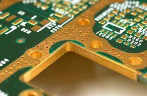
Printed Circuit Board Copper Plating is another important method for PCB board surface treatment:
In this process, all surface areas and drill holes are plated with copper, and some resist is poured on the unneeded copper surface, and then an etching resist metal is plated.
Even for a medium-sized printed circuit board, this requires an electric excavator that can provide a considerable amount of current to make an easy-to-clean, smooth and bright copper surface for subsequent processes.
If you don’t have a photoelectric plotter, you need to use a negative film to expose the circuit pattern, making it a more common contrast inversion dry film photoresist.
Etching the full-board copper-plated circuit board will remove most of the material plated on the circuit board again. As the copper carrier liquid in the etchant increases, the burden of additional corrosion on the anode is greatly increased.

Printed Circuit Board Copper Plating is another important method for PCB board surface treatment
Above Figure shows the printed circuit board plating flow chart of the removal process.
For the manufacture of printed circuit boards, circuit plating is a better method, and its standard thickness is as follows:
1) Copper
2) Tin-lead (circuits, pads, through holes)
3) Nickel 0.2mil
4) Gold (top of connector) 50μm
The reason why such parameters are maintained in the electroplating process is to provide high conductivity, good solderability, and high mechanical strength to the metal plating layer, and can withstand the terminal panel of the components and fill copper from the surface of the circuit board into the plated through hole.


