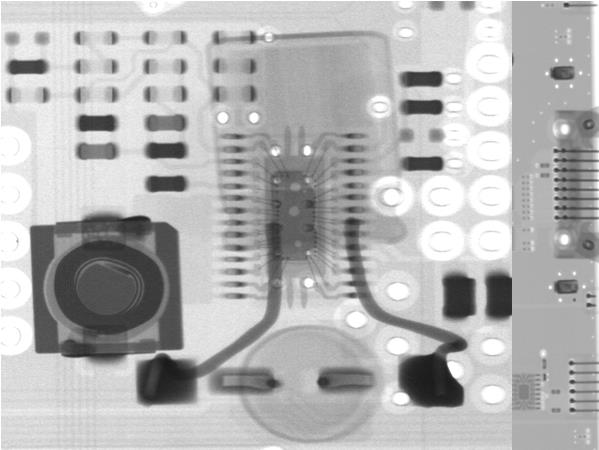
PCB board Reverse engineering technology is used to research or repair electronic equipment without schematic diagrams, such as electronic PCB board repair unit or imported automatic control system circuit board with partial schematic diagram maintenance, can also be used for teaching, scientific research, especially for those technology development company to research on the method of the device application or the implementation of the new technology standard, as well as the detailed analysis of the hardware circuitry and functionality when the imported electromechanical equipment or instrument is localized.

PCB Reverse Engineering Technology technology is also of value in the field of PCB design. It can be used to verify the correctness of manual layout and wiring. This is the subject of the current EDA (Electronic Design Automation) software.
The automatic layout technology of the schematic diagram has similarities with the automatic routing technology of the hybrid tuner PCB board design software. The research of this technology is also beneficial to further develop the domestic EDA software package with independent property rights.


