

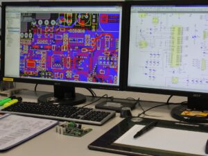
The Printed Circuit Board layout is optimized in terms of grounding, decoupling, and signal routing and can be used as a model when laying out the ADC section of the PC board in a system. The actual evaluation board layout is usually available from the ADC manufacturer in the form of Printed Wiring Board CAD files (Gerber files).
La técnica de ingeniería inversa de la placa PCB implica extraer información de una PCB existente para comprender cómo funciona, identificar sus componentes, rastrear las conexiones y reconstruir su diseño esquemático.
In many cases, the printed circuit board layout of the various layers appears on the data sheet for the device. It should be pointed out, though, that an evaluation board is an extremely simple system. While some guidelines can be inferred from inspection of the layout, the system that you are designing is undoubtedly more complicated. Therefore, direct use of the layout may not be optimum in larger systems.
تتضمن تقنية الهندسة العكسية للوحة ثنائي الفينيل متعدد الكلور استخراج المعلومات من ثنائي الفينيل متعدد الكلور الموجود لفهم كيفية عمله وتحديد مكوناته وتتبع الاتصالات وإعادة بناء تصميمه التخطيطي.
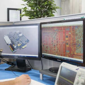
Manufacturers of high performance mixed-signal ICs, like Analog Devices, often offer evaluation boards to assist designers in their initial evaluations and PC Board layout. ADC evaluation boards generally contain an on-board low jitter sampling clock oscillator, output registers, and appropriate power and signal connectors. They also may have additional support circuitry such as the ADC input buffer amplifier and external reference.


