Since the sensitivity of electronic equipment is getting higher and higher, which requires the anti-interference ability of the equipment to become stronger and stronger, Therefore, Reverse Engineering PCB to Reduce Noice and Electromagnetic Inteference has become more difficult. How to improve the anti-interference ability of PCB has become one of the key issues that many engineers pay attention to. This article will introduce some tips for reducing noise and electromagnetic interference in PCB reverse engineering:

Here are 24 tips for reducing noise and electromagnetic interference through PCB reverse engineering after years of designing:
1, can use low-speed chips without high-speed, high-speed chips used in key places.

2, the string can be used to reduce the jump rate of the upper and lower edges of the control circuit.
3, Try to provide some form of damping for relays, etc.
4, Use the lowest frequency clock that meets the system requirements.
5, The clock generator is as close as possible to the device. The quartz crystal oscillator housing should be grounded;
6, Circle the clock area with the ground wire and keep the clock track as short as possible.
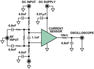
7, I / O drive circuit as close as possible to the edge of the printed board, let it leave the printed board as soon as possible. The signal entering the printed board should be filtered, and the signal from the high-noise area should be filtered. At the same time, the signal of the string termination is used to reduce the signal reflection.
8, MCD useless terminal to be connected, or grounded, or defined as the output, the end of the integrated circuit on the power supply must be connected, do not hang.
9, Do not leave the input terminal of the unused circuit. The unused input terminal is grounded and the negative input is connected to the output terminal.
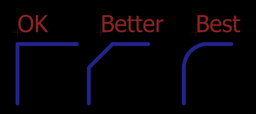
10, The printed circuit board uses 45 degree fold lines instead of 90 degree lines as far as possible to reduce the external transmission and coupling of high frequency signals.

uses 45 degree fold lines instead of 90 degree lines


