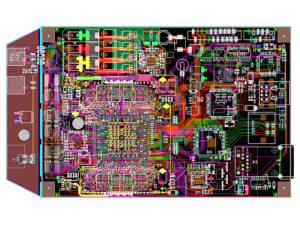
High Density Printed Circuit Board Design Global Trend
Most people think the BALL GRID ARRAY package with mass chip scale as a feasible solution for portable electronic product to break the space limitation for High Density Printed Circuit Board Design. And it will simultaneously satisfy both the requirement for more complicate functions and performance. However the design high density circuit board of portable electronic product process should take the assembly into account.
When developing electronic products for today’s value-driven markets, performance and reliability are top priorities. In order to compete in this market, developers must also pay attention to the efficiency of assembly because it can control manufacturing costs.

high density pcb design
Technological advances and the ever-increasing complexity of electronic products are creating a need for higher density printed circuit board fabrication methods. When designing surface-mount, fine-pitch, and vector-packaged integrated circuits, high density printed circuit boards with finer line widths and thinner spacing may be required.
However, looking to the future, some companies that are already supplying miniature via holes and serially assembled circuit boards are investing heavily to expand their capabilities. These companies recognize the current trend of electronics for smaller packages. The communications and personal computing industry alone is enough to lead the global market.


