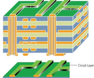
Except double layers PCB Board, 4 layers PCB board is also very hot subject in the electronic world, in fact, 4 layers PCB board copying stands for two double-sided boards duplication, and 6 layer PCB board copying means replicate three double-sided PCB boards….
The reason why multiple layers PCB Board copying are daunting is because we can’t see the internal circuitry pattern. The most effective way to get the knowledge of its internal layer of sophisticated multilayer board is DELAYERING.

multilayer pcb board delayering
There are many ways to solve the problem of de-layering, such as chemical solution corrosion, peeling tools, brutal force such as scrubbing etc., but it is easy to over-score the layers which could probably damage some of the copper tracks, missing copper track or hole, extra/missing holes or pads. According to our experience that scrubbing the layer by sand paper is the most accurate and secure way.

scrub pcb copper track
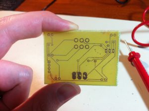
When copying the top or/and bottom layer of the PCB, we usually use sandpaper to polish the top or bottom layer to expose inner layer.
Place target PCB board on an even platform, then hold the sandpaper and rub evenly on the PCB surface (if the board is small, you can also tile the sandpaper and use a finger to hold the PCB and rub on the sandpaper). The point is to ensure the PCB has been place evenly so that you can scrubbing can executing properly.
Silk screen printing and solder resist mask are easier to be wiped off, and the copper wire and copper film must be wiped properly.


