Reverse Engineering Circuit Board Implementation Process mainly includes the following aspects.
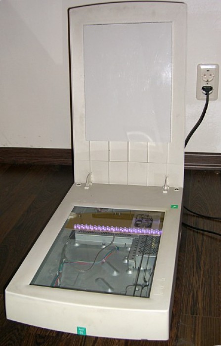
First, scan the circuit board that needs to be reverse engineered and record the position of all components on the circuit board, disassemble all the components to make a bill of materials, and arrange the personnel to purchase the components according to the BOM list.

Then scan the blank printed circuit board and use PCB design software processes the scanned image to obtain the original pcb layout drawing, gerber file and schematic diagram;
Finally, the PCB layout design and purchased components are sent to the PCB Board manufacturing company for PCB production, the electrical connection of the components are completed, and the circuit board is tested and debugged, thus completing the printed circuit board copying of the products on the market, thereby saving the economy, R&D costs and shortened production cycle.


