When a printed circuit board (PCB) fails, the absence of a schematic diagram can turn troubleshooting into a puzzle. However, innovative techniques and systematic approaches can help technicians recover malfunction PCB card systems even without a roadmap. Below is a fresh guide to diagnosing and repairing complex PCB issues when schematics are unavailable.
1. Understand the PCB’s Functional Context
Before diving into repairs, gather clues about the PCB’s role:
-
Identify the device’s purpose – Is it part of a power supply, communication module, or control system?
-
Research similar PCBs – Look for datasheets or repair manuals of comparable boards.
-
Label key components – Note the positions of ICs, connectors, and power regulators to infer circuit flow.
This contextual analysis helps prioritize testing areas and narrow down potential failure points.
1. Comprender el contexto funcional de la PCB
Antes de comenzar las reparaciones, investigue la función de la PCB:
Identifique la función del dispositivo: ¿Forma parte de una fuente de alimentación, un módulo de comunicación o un sistema de control?
Investigue PCB similares: busque hojas de datos o manuales de reparación de placas similares.
Etiquete los componentes clave: observe la posición de los circuitos integrados, conectores y reguladores de potencia para inferir el flujo del circuito.
Este análisis contextual ayuda a priorizar las áreas de prueba y a delimitar los posibles puntos de fallo.
2. Leverage Advanced Diagnostic Tools
While multimeters are essential, modern tools can accelerate the process:
-
Thermal Imaging Cameras – Detect hotspots caused by short circuits or overloaded components.
-
X-Ray Inspection – Reveal hidden defects like cracked vias or internal trace damage (common in multilayer PCBs).
-
Component Testers – Use dedicated LCR meters or transistor testers for accurate passive/active component analysis.
These tools reduce guesswork, especially when schematics are missing.
3. Adopt a Divide-and-Conquer Approach
Break the PCB into functional blocks to isolate faults:
-
Power Section – Test voltage regulators, diodes, and capacitors for stable output.
-
Signal Paths – Follow input/output lines (e.g., from sensors to microcontrollers) using an oscilloscope.
-
Clock Circuits – Verify oscillators and crystal resonators for correct frequency output.
By compartmentalizing the board, you can focus on one subsystem at a time.
3. Adottare un approccio “dividi et impera” Scomponi il PCB in blocchi funzionali per isolare i guasti: Sezione di potenza – Testa regolatori di tensione, diodi e condensatori per un’uscita stabile. Percorsi del segnale – Segui le linee di ingresso/uscita (ad esempio, dai sensori ai microcontrollori) utilizzando un oscilloscopio. Circuiti di clock – Verifica la corretta frequenza di uscita degli oscillatori e dei risonatori a cristallo. Compartimentando la scheda, è possibile concentrarsi su un sottosistema alla volta.
4. Reverse Engineer Critical Subcircuits
While fully reverse-engineering a PCB is time-consuming, targeting high-risk areas saves effort:
-
Power Rails – Trace connections from the input port to voltage regulators and decoupling capacitors.
-
Reset Circuits – Identify components tied to IC reset pins (often involving resistors, capacitors, or diodes).
-
Communication Lines – Map UART, SPI, or I2C pathways using pinout references for known ICs.
Documenting these subcircuits creates a partial schematic for future reference.
5. Exploit Signal Injection and Probing
Stimulate the PCB to observe responses:
-
Inject Test Signals – Use a function generator to input waveforms into analog circuits (e.g., audio amplifiers).
-
Monitor Outputs – Check for expected signal amplification or filtering using an oscilloscope.
-
Bypass Suspected Components – Temporarily replace a damaged section with external circuitry to validate functionality.
This method is particularly effective for analog or mixed-signal boards.
6. Address Common Failure Patterns
Certain issues recur across PCBs. Prioritize checks for:
-
Failed Voltage Regulators – Output voltage discrepancies often stem from faulty regulators or blown fuses.
-
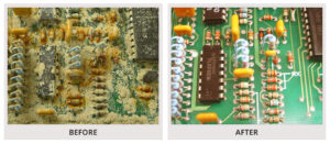
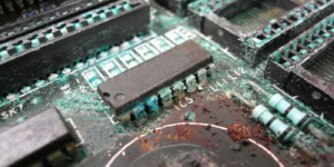
Corroded Traces – Common in humid environments; repair with jumper wires or conductive epoxy.
-
EEPROM/Flash Corruption – Reprogrammable ICs may require firmware reflashing if data is corrupted.
7. Build a Troubleshooting Framework
Create a repeatable process to recover malfunction PCB card systems efficiently:
-
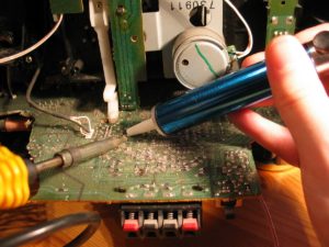
Document Every Step – Take photos, label components, and record measurements.
-
Prioritize High-Risk Areas – Focus on power sections and heat-sensitive components first.
-
Validate Repairs Incrementally – Test after each fix to avoid masking secondary faults.
Case Study Example
A industrial motor control PCB failed abruptly. With no schematic, the technician:
-
Mapped the power section and found a shorted MOSFET.
-
Used thermal imaging to locate an overheating voltage regulator.
-
Discovered corroded traces near the board’s edge connector.
After replacing the MOSFET, regulator, and repairing traces, the PCB functioned normally.
Conclusion

5. Используйте ввод сигнала и зондирование Стимулируйте печатную плату для наблюдения за реакциями: Ввод тестовых сигналов — используйте генератор функций для ввода сигналов в аналоговые схемы (например, аудиоусилители). Мониторинг выходов — проверьте ожидаемое усиление или фильтрацию сигнала с помощью осциллографа. Обход подозрительных компонентов — временно замените поврежденный участок внешней схемой для проверки работоспособности. Этот метод особенно эффективен для аналоговых или смешанных сигнальных плат.
Recovering a malfunctioning PCB card without schematics demands creativity, advanced tools, and structured problem-solving. By combining functional analysis, subcircuit reverse-engineering, and targeted signal testing, technicians can breathe life into seemingly irreparable boards. The key lies in methodically isolating faults rather than relying on trial-and-error. With these strategies, professionals can consistently recover malfunction PCB card units, minimizing downtime and fostering sustainable electronics repair practices.
It is commonly known that recover PCB card needs to use a schematic diagram in most of the cases, particularly when the broken PCB card is complicated and comes from the application unfamiliar with repairing engineer, even if the engineer has acumulated sufficient amount of experience from previous work, he won’t be able to fix this issue promptly and effortlessly, hereby we list some of the main principles that can be followed when try to recover PCB card to increase the working efficiency:
Recover PCB Card in the absence of Schematic Diagram
Inspect and recover PCB Card from internally to externally by using the online rework station, if the circumstance is allowable, it is better to use a proper functional PCB Card to compare the defected one, and use twin rod VI curve scanning functions to make the comparison, and the comparison point can start from the terminal then slowly and steady spread into the other area especially the comparison on the capacitors, can recover the disadvantage of multimeter which can not measure if there is any leakage on the electro-capacitor online;