

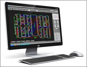
Printed circuit board design are by far the most common method of assembling modern electronic circuits. Comprised of a sandwich of one or more insulating layers and one or more copper layers which contain the signal traces and the powers and grounds, the design of the layout of Printed circuit board design can be as demanding as the design of the electrical circuit.
Printed circuit board (PCB) design is the most widely used method for assembling modern electronic circuits, providing a reliable, compact, and scalable solution for integrating electrical components. PCBs are composed of one or more insulating layers combined with one or more copper layers that contain signal traces, power connections, and ground planes. The design and layout of a PCB can be just as challenging as designing the electrical circuitry itself, requiring careful planning to ensure functionality, signal integrity, and manufacturability.
Das Design von Leiterplatten (PCB) ist die am weitesten verbreitete Methode zur Herstellung moderner elektronischer Schaltungen und bietet eine zuverlässige, kompakte und skalierbare Lösung für die Integration elektrischer Komponenten. Leiterplatten bestehen aus einer oder mehreren Isolierschichten und einer oder mehreren Kupferschichten, die Signalleitungen, Stromanschlüsse und Masseflächen enthalten. Design und Layout einer Leiterplatte können ebenso anspruchsvoll sein wie die Entwicklung der elektrischen Schaltung selbst und erfordern sorgfältige Planung, um Funktionalität, Signalintegrität und Herstellbarkeit sicherzustellen.
Understanding PCB Layer Structures and Component Mounting
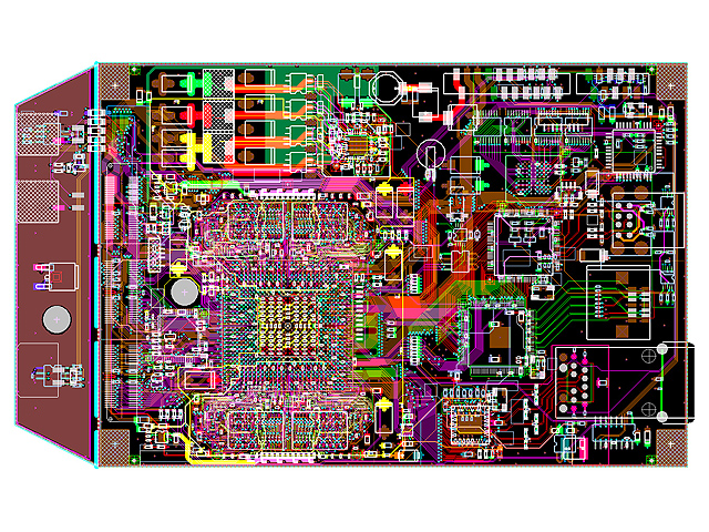
Most modern PCBs use a multilayer design, typically ranging from two to eight layers, though more complex systems may incorporate ten or more layers to accommodate high-speed signal routing and power distribution. These layers allow for better electromagnetic interference (EMI) control, improved heat dissipation, and greater signal integrity, especially in applications involving high-frequency circuits, embedded systems, and industrial automation.
Traditionally, PCB components were mounted using through-hole technology (THT), where component leads extend through drilled holes in the board and are soldered onto copper pads on the opposite side. While through-hole components provide strong mechanical bonds and are still used in power electronics and aerospace applications, modern PCB designs now rely heavily on surface-mount technology (SMT). SMT components are soldered directly onto the PCB surface without the need for drilled holes, allowing for smaller, lighter, and more complex circuit designs.
Traditionnellement, les composants de circuits imprimés étaient montés à l’aide de la technologie de montage traversant (THT), où les broches des composants traversaient des trous percés dans la carte et étaient soudées sur des pastilles de cuivre sur la face opposée. Si les composants traversants offrent des liaisons mécaniques solides et sont toujours utilisés dans l’électronique de puissance et l’aérospatiale, les conceptions de circuits imprimés modernes reposent désormais largement sur la technologie de montage en surface (CMS). Les composants CMS sont soudés directement sur la surface du circuit imprimé sans perçage, ce qui permet des circuits plus petits, plus légers et plus complexes.
Key Considerations in PCB Design
A well-designed printed circuit board ensures reliable electrical performance while optimizing manufacturing efficiency. Key factors in PCB layout design include:
-
Component Placement: Proper arrangement of components minimizes trace lengths, reduces noise, and improves heat dissipation.
-
Power and Ground Planes: Dedicated power and ground layers help maintain voltage stability and reduce electromagnetic interference (EMI).
-
Signal Routing: High-frequency signals require careful routing techniques, such as impedance matching and controlled differential pair routing.
-
Thermal Management: Components generating significant heat require heat sinks, vias, or dedicated cooling strategies to prevent performance degradation.
-
Manufacturability: Ensuring that the Gerber files, BOM list, and schematic diagram match the design specifications reduces the risk of errors during fabrication.
Conclusion
Understanding the principles of printed circuit board design is crucial for engineers, designers, and manufacturers who aim to create high-performance electronic systems. Whether designing a simple two-layer PCB or a complex multilayer circuit board, following best practices in component placement, signal integrity, and power distribution ensures a functional and efficient PCB design that meets modern industry standards.
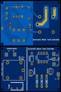
Most modern systems consist of multilayer boards of anywhere up to eight layers (or sometimes even more). Traditionally, components were mounted on the top layer in holes which extended through all layers. These are referred as through hole components.
More recently, with the near universal adoption of surface mount components, you commonly find components mounted on both the top and the bottom layers. The design of the Printed circuit board can be as important as the circuit design to the overall performance of the final system.
clonare il file gerber della scheda elettronica PCB, il disegno del layout e l’elenco delle distinte base, il diagramma schematico del reverse engineering del circuito stampato;
We shall discuss in this chapter the partitioning of the circuitry, the problem of interconnecting traces, parasitic components, grounding schemes, and decoupling. All of these are important in the success of a total design.
Printed circuit board effects that are harmful to precision circuit performance include leakage resistances, IR voltage drops in trace foils, vias, and ground planes, the influence of stray capacitance, and dielectric absorption (DA).
نسخ لوحة الدوائر المطبوعة على الوجهين واستنساخ ملف جربر لثنائي الفينيل متعدد الكلور، وتصميم التخطيط، والتخطيطي؛ النظام الإلكتروني للوحة الدوائر الهندسية العكسية وتحسين نظام التصميم لجعل لوحة PCB بأداء أفضل ؛
In addition, the tendency of PCB board design to absorb atmospheric moisture (hygroscopicity) means that changes in humidity often cause the contributions of some parasitic effects to vary from day to day.


