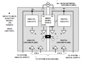
An alternative grounding method for a mixed-signal device with high levels of digital currents in Multilayer Board Reverse is shown in below Figure. The AGND of the mixed signal device is connected to the analog ground plane, and the DGND of the device is connected to the digital ground plane.

High DC Multilayer Board reverse
The digital currents are isolated from the analog ground plane, but the noise between the two ground planes is applied directly between the AGND and DGND pins of the device. For this method to be successful, the analog and digital circuits within the mixed signal device must be well isolated. The noise between AGND and DGND pins must not be large enough to reduce internal noise margins or cause corruption of the internal analog circuits.
Above Figure shows optional Schottky diodes (back-to-back) or a ferrite bead connecting the analog and digital ground planes. The Schottky diodes prevent large dc voltages or low frequency voltage spikes from developing across the two planes.
These voltages can potentially damage the mixed-signal IC if they exceed 300 mV because they appear directly between the AGND and DGND pins. As an alternative to the back-to-back Schottky diodes, a ferrite bead provides a dc connection between the two planes but isolates them at frequencies above a few MHz where the ferrite bead becomes resistive.
This protects the IC from dc voltages between AGND and DGND, but the dc connection provided by the ferrite bead can introduce unwanted dc ground loops and may not be suitable for high resolution systems.


