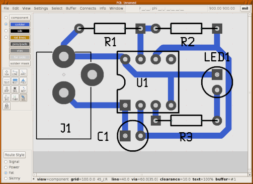
Engineer can use Altium Designer to Design PCB Board Drawing.
First, design the schematic diagram. You need to master the knowledge of circuitry pattern, digital and analog. It is not realistic to design a circuit diagram completely from scratch. You can design the circuit you need by referring to the information on the Internet.
Some devices do not have their own library, you have to draw the principle library.
Second, draw the package library. You need to draw a package library that meets the requirements based on the size of the device in the Datasheet. This part takes more time and is crucial. If the drawing is wrong, the device cannot be soldered by hand.
Again, generate the PCB layout drawing or gerber file from the schematic. At this point, the PCB diagram shows the package for each device and their connections. The wires are flying lines and it looks dazzling.
You need to replace each flying wire with a continuous wire. This is called wiring. Before the wiring layout, set the rules, arrange the position of each device reasonably, and then follow the certain principles (mainly for the stability of the work, these wiring principles are a lot of information on the Internet), and you can try the new layout or Pin configuration. This step often takes the most part of the time.

Finally, some details. For example, prevent mounting holes, adjust silk screen layers, floor, rule checks, and more. A PCB board was successfully drawn. Then soldering, debugging, testing, everything is normal, only to complete the drawing of a qualified PCB board. I suggest you borrow a book about Altium Designer (or other software), do it on the screen, or look at other people’s video tutorials online, maybe save some time.


